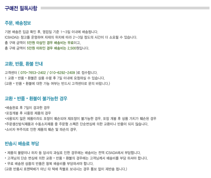
| |
 IC
> 메모리
> RAM
> GLT5160L16 IC
> 메모리
> RAM
> GLT5160L16
최소주문수량 : 10개
|
|
|
|
| 제조회사 : G-LINK |
| 판매가격 : 3,000원 |
|
|
|
| 적립금액 : 0원 |
|
|
|
|
|
| ★★★★★ |
| 신속하고 정확한 배송을 약속드립니다 |
|
|
|
|
|
FEATURES
Single 3.3 V ±0.3 V power supply
Clock frequency 100 MHz / 125 MHz / 143 MHz/
166 MHz
Fully synchronous operation referenced to clock rising edge
Dual bank operation controlled by BA (Bank Address)
CAS latency- 2 / 3 (programmable)
Burst length- 1 / 2 / 4 / 8 & Full Page (programmable)
Burst type- sequential / interleave (programmable)
Industrial grade available
Byte control by DQMU and DQML
Column access - random
Auto precharge / All bank precharge controlled by A[10]
Auto refresh and Self refresh
4096 refresh cycles / 64 ms
LVTTL Interface
400-mil, 50-Pin Thin Small Outline Package (TSOP II) with
0.8 mm lead pitch
60-Ball, 6.4mmx10.1mm VFBGA package with 0.65mm Ball
pitch & 0.35mm Ball diameter.
데이터시트 보기
* 본 제품은 경우에 따라 호환되는 타사 제품으로 변경될 수 있음을 알려 드립니다.
주문시 참고 하세요~~ |
* 제품 사용 전 반드시 테스트 후 사용하시기 바랍니다.
* 첨부된 데이터시트는 참고용으로만 사용하시기 바랍니다. |
 |
|


